Electroplating of copper for semiconductor package interconnects
Delivering the next generation of Package
As Moore’s Law reaches its physical limits in the front-end, transistor level, manufacturing, advances in chip performance rely more on back-end miniaturization, particularly in packaging. (1) Advanced packaging technologies, such as 3D integrated circuits (ICs), enable higher component density, improved power performance, and enhanced input/output (I/O) signal transmission. These qualities are essential for applications in autonomous vehicles, the internet of things (IoT), and artificial intelligence (AI). A key element in packaging is the electrical connection between dies and other components, typically in form of copper interconnects.
Types of Copper Interconnects in Semiconductor Packaging
At the packaging level, representative interconnects include Through-Silicon Vias (TSV), redistribution layers (RDLs) and Fan-Out Wafer-Level Packages (FOWLPs). TSVs are copper wires, with typical diameter of 1-10 µm and length between 10 and 150 µm, that pass vertically through a silicon wafer enabling chip-to-chip connections in 3D multi-chip stacks. For lateral connections, RDLs are used with copper wiring layers with typical width and thickness starting from 5 µm. In contrast to Fan-In Wafer Level Connections (FIWLC), which includes interconnects within the die (wafer) area, FOWLPs provide a structured wiring solution between various semiconductor components such as logic and memory chips, multiple dices, or chips and printed circuit board (PCB). This interconnect methods consist of RDLs, copper pillars and micro bumps, usually with diameters in the range of 10 and 50 µm.
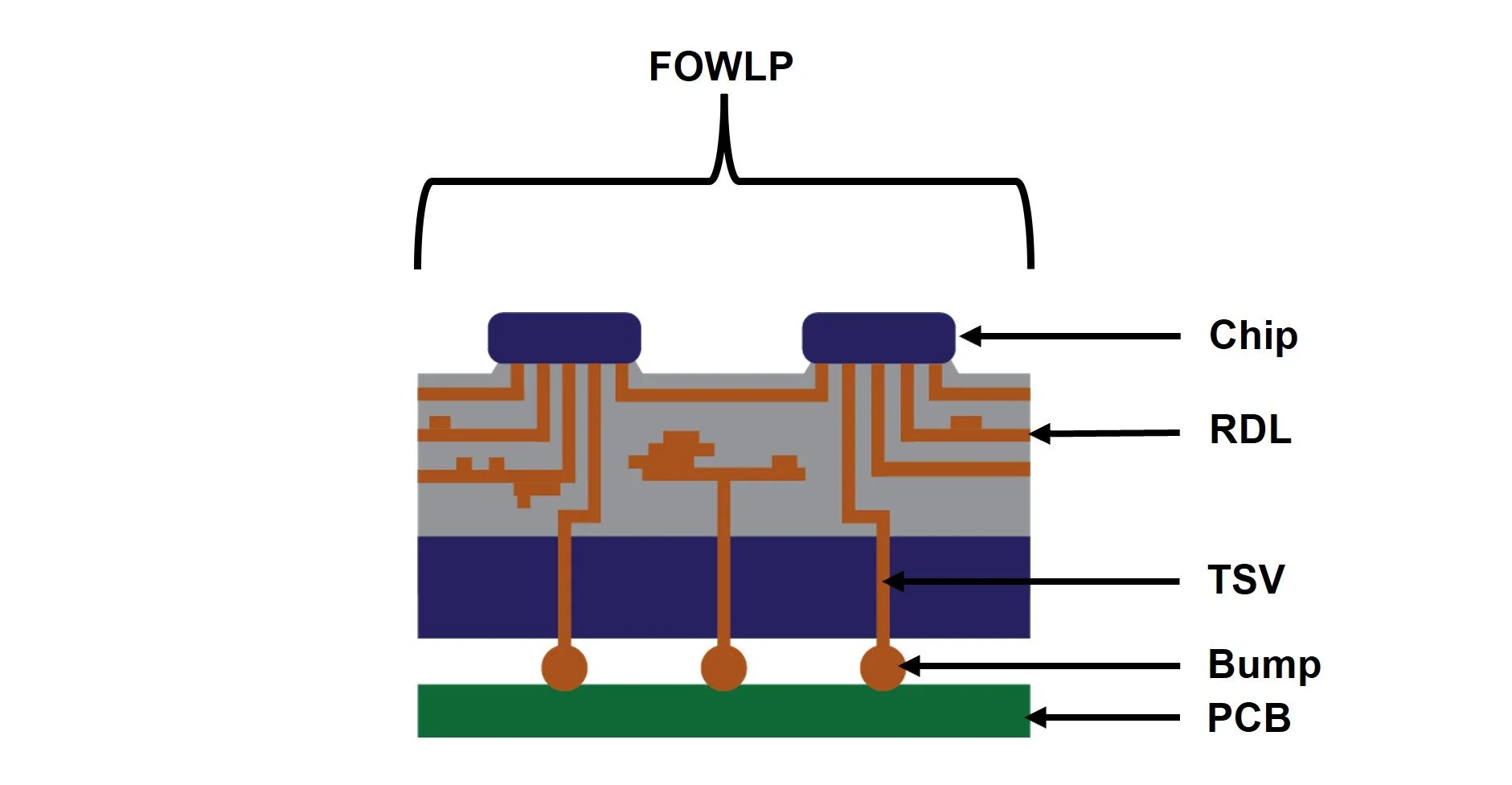
Image 1: Simplified not-to-scale visualization of Fan-Out Wafer-Level Package (FOWLP), Redistribution Layers (RDLs), Through-Silicon Vias (TSVs).
Additives for Challenges in Copper Electroplating
Copper electroplating from acidic sulphate electrolyte is the primary method for manufacturing microelectronic interconnections. A mask on top of the seed layer defines the exposed areas for the interconnect structures. In the through-mask plating process, electroplating only takes on areas of the seed layer that are not covered by the mask. In Damascene plating, in contrast, a seed layer is deposited over a patterned material and the plated metal covers the entire surface. The electroplating process is associated with challenges, including void-free filling of the small-scale high aspect ratio features present in the mask and minimizing grain boundary defects that can compromise thermomechanical stability. (2) By adjusting the content of organic plating additives in the electrolyte the two challenges can be successfully addressed. Additives are grouped into the categories of accelerators, suppressors, and levellers, each of them playing a distinct function in modulating the electrodeposition rate at the opening and bottom environments of the patterned feature. (3) The ideal filling approach, known as superconformal filling, ensures bottom-up copper deposition in micro scaled features. (4) For defect-free filling, a higher deposition rate in the bottom than on the sides of the feature is required. Accelerator compounds such as bis(sodium sulfopropyl)disulfide (SPS) with thiol and sulfonate groups enrich at the bottom of vias and trenches. (5, 6) In the synergistically presence of chloride ions with SPS, the copper electrodeposition is strongly accelerated. (7, 8) Suppressors, often based on polyether compounds such as polyethylene glycol (PEG), form PEG-Cl- or PEG-Cu+-Cl- complex layer onto the cathode surface, which increases the charge-transfer resistance and thus, inhibits the electroplating of copper. (9, 10, 11) Levelling agents are typically cationic nitrogen-containing polymers or heterocyclic compounds (example: PEI: Polyethyleneimine) with a positive charge in acidic solutions. (12, 13) The positively charged nitrogen-based functional groups of levellers are electrostatically attracted to preferentially adsorb on the protrusions of the substrate on which the current density is highest. This selective adsorption increases the local overpotential, inhibiting copper deposition on protrusions and promoting a more uniform surface. The additives composition in the plating electrolyte is optimized to ensure copper is uniformly deposited in the fine prepatterned features of TSVs and RDLs.
Industrial Scale Equipment for Copper Electroplating
The most prominent equipment providers for electrochemical deposition systems in advanced packaging are Applied Materials Inc. and Lam Research Inc. Applied Materials has developed the Applied Raider® Edge ECD (electrochemical deposition), which supports manufacturing processes on wafer sizes at 150, 200 and 300 mm and enables various processes, including cleaning, plating and etching a wide range of metals. (14) This system is capable of producing relevant packing interconnects including TSVs, RDLs, and micro bumps, and thus suitable for FAWLP application in industry. The raider platform competes with Lam Research 3D SABRE. (15), originally developed by Novellus. The SABRE system is designed for high-throughput electroplating, facilitating the formation of conductive bumps, RDLs, TSVs in wafer-based manufacturing environments.

Image 2: Visualization of the increased processing areas for a transition from traditional wafer sized to panel sized manufacturing.
Beyond Wafer size: Panel-Level Packaging
The continuation of the substrate scaling from 300 mm circular-shaped wafers towards larger substrates brought forth rectangular panels with sizes of 515 mm x 510 mm and 600 mm x 600 mm. (16) For panel-level packaging (PNP), manufacturing equipment and processes have to be adapted to match panel dimension, which increases the processed areas by 3 to 6 times to multiply the number of chips produced. Semsysco GmbH developed and patented a high speed and high uniformity plating process, which is applicable for panel sized substrates. This process employs a special tool that injects the copper-ion-rich electrolyte in close proximity to the substrate surface complemented by electrolyte removal holes to ensure a direct path to the anode. (17) This tool establishes a uniform electrical field and mass transport across the large substrate surface, enabling that the plating process yields a uniform height distribution of the plated copper pillars electroplated within the vias and trenches in the photoresist material covering the substrate. (18) The technology ensures minimal height deviation between copper features at the centre and edges of the substrate. Recognizing the potential of this innovation, Lam Research acquired Semsysco GmbH was acquired in 2022 to further advance its electroplating and processing capabilities for next-generation of panel packaging solutions.
In the near future, back-end solutions such as advanced interconnects and panel-level packaging will play a pivotal role in sustaining the semiconductor manufacturing industry’s progress. Ongoing innovation in electroplating technology and process optimization will be crucial in meeting the demands of next-generation electronic devices.