Extending Moore’s Law with Carbon Nanotubes in Complementary Transistor Architecture
Innovation in Transistor Technology
Moore’s Law, predicting that the number of transistors on a chip would double approximately every two years, has propelled innovation in semiconductor nanoscience. Originally an observation by Intel co-founder Gordon Moore, this trend became an incentivizing guiding principle for shrinking the size of transistors. However, complementary metal-oxide semiconductor (CMOS) technology, which has been prevailing in manufactured microchips, has approached its physical limits. Further downsizing of the transistor size in the traditional CMOS arrangement of transistors, side by side on a planar wafer, raises the probability of quantum tunnelling from source to drain when the transistor is in OFF state and thus leads to error in computations. To continue scaling according to Moore’s Law, the semiconductor industry has transitioned to vertical transistor structures, such as FinFET and Gate-All-Around FET (GAAFET) designs. Beyond these novel transistor architectures, materials innovation is ongoing for further miniaturization and performance improvement. One promising material class are semiconducting carbon nanotubes (s-CNT), which have the potential to scale the gate length beyond silicon’s limits.
Classification of carbon nanotubes by electrical properties
Carbon nanotubes can be categorized into multi-wall (MWCNTs) and single-wall (SWCNTs) based on the amount of layers in tubular shape within each other. MWCNTs generally behave as metallic conductors at room temperature, while SWCNTs exhibit a broader range of electronic properties, behaving as either metallic or semiconducting depending on their chirality. (1) The electronic properties of an SWCNT are determined by its atomic arrangement, defined by the chiral vector, which describes the direction, in which a graphene sheet is rolled up to the carbon nanotube as shown in Image 1 a. (2) Depending on the chiral index pair SWCNTs can be classified as zigzag, armchair, or chiral. Armchair SWCNTs are always metallic (1 b), chiral (1 c) and zigzag (1 d) can be either metallic or semiconducting. Since their chirality dictates their electronic properties, it determines their viability for use in transistors. Only semiconducting SWCNTs are suitable contenders as gate for application in future transistors. (3, 4, 5)

Image 1: a) Chirality of SWCNTs as a function of chiral indexes (n, m). Prepared with Nanotube Modeler, JCrystalSoft.
The first carbon nanotube transistor
Semiconducting SWCNTs possess a well-defined one-dimensional structure and exceptional charge transport properties, enabling quasi-1D ballistic transport. (6) They also have the potential to be ten times more energy-efficient than conventional metal oxide semiconductors due to lower operating voltage (7), making them a strong candidate for next-generation of CMOS transistor technology. The first carbon nanotube field-effect transistor (CNTFET) was demonstrated in 1998, utilizing a SWCNT as the channel material. (8) This early CNTFET design featured a 300-nm layer of thermally grown SiO2 on a silicon substrate, with the SWCNT connected to three platinum (Pt) electrodes. By applying a voltage to the gate electrode, the SWCNT could be switched between conducting and insulating states, similar to a traditional MOSFET. This proof-of-concept demonstrated that s-CNTs could function as transistor channels. The scaling of the channel length led to the first sub-10 nm CNTFET, which delivered double the on-current at low operating voltages compared to silicon reference transistors. (9)
Carbon nanotube transistor with a 5 nm gate length
The physical gate length of silicon-based CMOS transistors has been scaled down to 5 nm in laboratory settings. However, miniaturization below 10 nm lead to reliability issues caused by quantum tunnelling, which results in leakage currents. (10, 11) To compare the performance with silicon technology and to explore the physical limits of the CNTFET technology, a research team led by Zhiyong Zhang and Lian-Mao Peng at Peking University prepared a top-gated CNTFET with a gate length of 10 and 5 nm. (12) The 10 nm CNT CMOS FETs operated at a lower supply voltage of 0.4 V compared to 0.7 V for silicon CMOS while maintaining higher performance. This is a crucial advantage since transistors scaling aims to reduce supply voltage while preserving or improving performance. A key performance metric in transistors is the subthreshold slope (SS), which measure how effectively the gate controls the channel. In long channel-devices, an ideal SS value is around 60 mV/decade, meaning that a tenfold increase in drain current requires at least a 60 mV increase in gate voltage. However, in ultra-short-channel FETs, short channel effects arise because the drain begins to influence the channel electrostatically, reducing gate control. For palladium-contacted 5 nm CNTFETs, SS values degraded to from 105 to 130 mV/decade. To counteract this, researcher introduced graphene contacts, which improved electrostatic gate control and reduced SS to 72 mV/decade, which is significantly better than the 208 mV/decade typical of silicon MOSFET at the same scale. Notably, the 5 nm graphene contacted CNTFET approached the quantum limit of FETs, demonstrating single-electron switching.
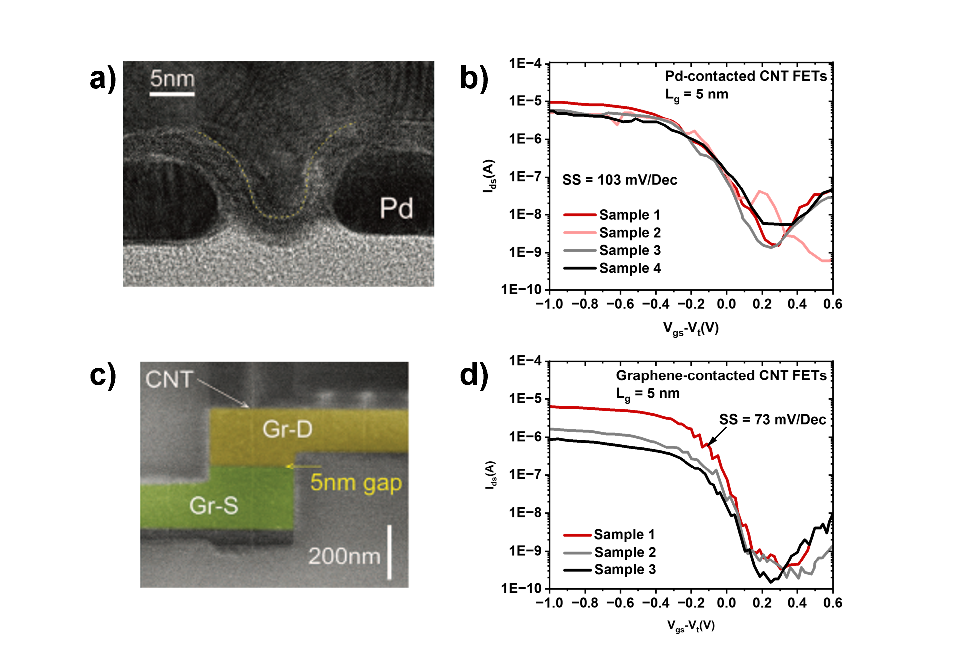
Image 2: a) TEM image of a normal Pd-contacted CNT FET with gate length of 5 nm. b) Transfer characteristics of four Pd-contacted CNT FETs with a gate length of 5 nm. c) SEM image of a graphene-contacted CNT FET with channel length of 5 nm, before deposition of the top gate electrode. d) Transfer characteristics of three typical graphene-contacted CNT FETs with a gate length of 5 nm. Reproduced from and replotted with data from (12).
Chip integration of carbon nanotube transistors
While prototype transistors with individual CNT have shown exceptional performance, scaling up to dense, chip-level integration remains a challenge. The primary hurdle to demonstrate large-scale CNT FETs based circuits is the precise alignment of a multitude of CNT on the wafer. In an upcoming article, I will explore how researcher are addressing this integration challenge to bring CNT transistors closer to commercial viability.